X-Ray Inspection for Electronics & Failure Analysis
A Service from our Failure Analysis Lab
Industry Challenges
- During the manufacturing process, parts, connections, and boards need to be verified to ensure proper assembly, functionality and high quality.
- Problems of intermittent failures start appearing in electronics products after entry into service.
- Detecting the root cause of these failures can be costly and time-consuming and may not always yield any deterministic results.
Our Solution
With our state-of-the-art equipment, we can help you inspect your products for defects and identify the root cause of failures.
- Advanced automatic 2D & 3D X-ray inspections to significantly help detect defects in a non-destructive, non-intrusive way.
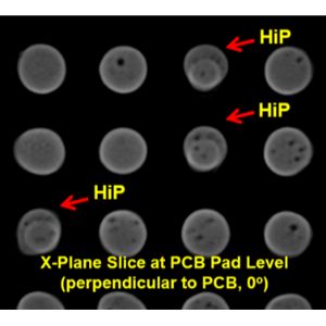
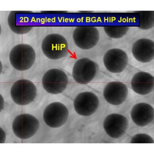
- X-ray inspection to reveal defects, whether hidden or visible, including open or shorted solder joints, lifted leads, voids, and unacceptable size variations in solder bumps (as in BGA components).
Key features:
- Up to 160kV, 10W
- 360° imaging, up to 35,500X magnification
- 2D live digital X-ray with < 100nm feature recognition
- CT technique to create slices in any plane of a PWB/PCB assembly without the need to cut the board
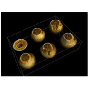
- 3D CT X-ray (Rotary; max sample size ~ 5.9” x 5.3”, max inspection area ~ 2.3” x 1.75”)
- 3D CT X-ray (X-Plane; provides high magnification CT reconstruction of target areas of PWB/PCBs)
- 29” x 22.8” maximum board size
- Automated BGA analysis


